A software company solving real metrology & inspection problems in semiconductor, display, and precision manufacturing — by uniting physics simulation, high-performance computing, industrial software, and industrial AI into one system.
// measurement → physics → compute → AI → report
fn haedosa(input: Signal) -> Solution {
    input.measure()
         .simulate()
         .learn()
         .verify()
}
“Haedosa” carries three layered meanings — expert, master, and navigator — that together describe how we work.
An expert who analyzes complex problems and proposes the solution.
A master who leads technical direction with deep insight and experience.
A navigator who explores unknown technical territory and charts new routes.
We can build the entire path ourselves — read measurement data, interpret it with physics models, process it at speed, and judge it with AI. Having all four under one roof is Haedosa's strength.
In-house optical analysis engine and first-principles computation for nanostructure spectra and inverse recovery.
GPU acceleration, streaming pipelines, and partition-based parallelism for real-time processing of massive inspection data.
High-precision, high-performance software engineered for field deployment — inspection compute optimization and takt-time tuning.
Context-based multi-class classification, diffusion-model anomaly detection, and virtual metrology.
OCD demands accurate physics, fast large-scale computation, and precise measurement-to-inverse recovery at once. From that origin, our technology evolved into three axes — and the same loop now extends to other metrology & inspection problems.
In-house physics simulation for structure analysis, model fitting, and virtual training-data generation.
Multicore parallelism and GPU acceleration that make large-scale simulation, image inspection, and ML feasible.
Specialized learning & inference — images, signals/spectra, numerical AI, and in-context inference — on advanced in-house engines.
Accurate metrology and simulation stay the reference; repeatedly accumulated data is learned to widen the speed, range, and adaptability of metrology & inspection — one signal modality at a time.
Prediction using simulation data with reference spectrum–structure pairs.
Multi-modal use of Raman + ellipsometry for structure & material analysis.
Linking process-sensor signals to metrology references for faster feedback.
Extending image-based inspection and metrology.
Reaching large-volume 3D signals such as holotomography.
Three layers: applications customers use directly, engines that own domain computation, and libraries that provide shared foundations across them.
Design, simulate, fit, generate data, train surrogates, and run Hybrid OCD inverse recovery — all in one desktop workbench, powered by fmmdosa's RCWA/FMM solver.
Labeling → training → evaluation → field deployment in one flow. Context-based multi-class classification, SAM auto-labeling, diffusion-model unsupervised anomaly detection.
GPU-accelerated holotomography volume rendering with cylinder fitting, surface-roughness measurement, and crack-size analysis in one workflow.
Reconstructs large-area surfaces from height-map tiles — overlap analysis optimization with CPU/GPU-accelerated parallel registration.
A Large Numerical Model approach: structured numerical tokens + autoregressive, in-context interpretation to estimate quality before physical metrology.
High-speed optical inspection for wafers and panels — holes/vias, surface defects, cavities, dimensions, bumps — with streaming + ROI parallelism and SPC export.
Decomposes development tasks by locality (ELD), recombines code/tests/docs through verified specs (LDD), and runs on-prem so secured data never leaves.
GPU-accelerated optical simulation: reflection/transmission, ellipsometry Ψ/Δ, Jones, Mueller, and Stokes S0–S7 — feeding spectrum libraries and numerical-AI training.
The shared ML engine. High-Precision Learning uses 2nd-order information for fast, accurate convergence on high-oscillation spectra — HPC makes data, HPL trains models.
Rigorous electromagnetic modeling of layered nanostructures — recovering geometry and optical response from measured spectra with production-grade accuracy.
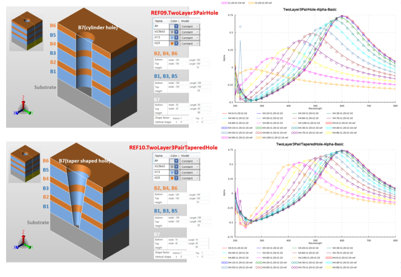
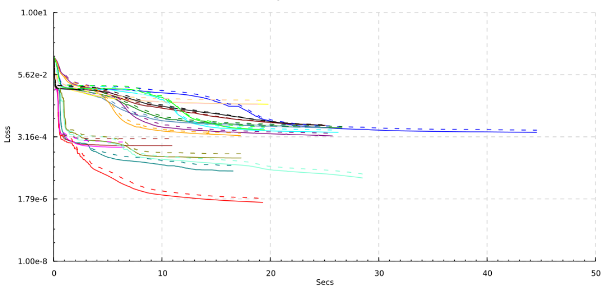
When the answer must be right to many digits, ordinary first-order training isn't enough. We use 2nd-order GPU-accelerated learning that drives loss to the precision floor — fast and reproducibly.
Founded in 2018 out of semiconductor OCD metrology-simulation work, building physics simulation, HPC, and industrial-AI solutions ever since.
Not a delivery checklist — cases where measurement & inspection data was processed faster, and physics simulation plus ML/AI was connected into field software.
OCD/SE optical engines, RCWA/FMM analysis, metrology-equipment software, high-precision ML — in-house engine, delivered software, Hybrid-OCD prediction research.
Analyzing existing inspection software, algorithm optimization, parallelization, CPU/GPU acceleration, takt-time improvement — meeting field requirements with drop-in modules.
AI-AOI classification, unsupervised anomaly detection, segmentation, factory-automation integration — field deployments and adapter systems.
Holotomography volume rendering, automatic geometry analysis, TGV/hole/bump inspection — GPU-accelerated 3D visualization and auto-metrology tools.
Tile registration of customer WLI data, CPU/GPU parallel processing, accuracy validation — faster large-area reconstruction with improved registration accuracy.
Spectrum analysis, wafer defect inspection, process/inspection data analysis — analysis and quality-judgment workflows built on accumulated data.
From initial consulting to full implementation, we navigate the complexity with you — and leave you with sustainable, reproducible solutions.