
Haedosa
Company & Technology Introduction — we chart a clear path through the sea of complex problems.
-- measurement → physics
-- → compute → AI → report
haedosa :: Principle
        -> Computation
        -> AI
        -> Problem
        -> Solution
haedosa p c ai challenge = solve
A software company for industrial metrology & inspection.
Semiconductor, display, and precision manufacturing need software that measures more accurately, inspects faster, and adapts to more product and process conditions. Haedosa unites physics simulation, HPC, industrial software, and industrial AI into one system — and accumulates each project's results as reusable numerical-AI capability.
HAEDOSAOne name, three roles.
Hae · 해
An expert who analyzes complex problems and proposes the solution.
Dosa · 도사
A master who leads technical direction with deep insight and experience.
Haedosa · 해도사
A navigator who explores unknown technical territory and charts new routes.
Four disciplines, one team.
Physics Simulation
In-house optical analysis & first-principles computation.
HPC
GPU acceleration & parallel processing for massive data.
Industrial SW
High-precision software built for field deployment.
Industrial AI
Classification, anomaly detection & virtual metrology.
HAEDOSAThree axes, learned from OCD.
Principle
In-house physics simulation for structure analysis, model fitting, and virtual training-data generation.
Computation
Multicore parallelism & GPU acceleration for large-scale simulation, inspection, and ML.
AI · Learning
Specialized image, signal/spectrum, numerical-AI, and in-context learning on in-house engines.
One repeatable improvement loop.
Optical spectra
Simulation + reference spectrum–structure pairs.
Raman
Raman + ellipsometry, multi-modal analysis.
Virtual metrology
Sensor signals linked to metrology references.
2D images
Image-based inspection & metrology.
3D volume
Large-volume 3D signals.
National R&D · OCD 2023–27 · Raman-SE 2024–26Applications · engines · libraries.
Software in the field today.
Design, simulate, fit, generate data, train surrogates, and run Hybrid OCD inverse — one workbench on fmmdosa.
Label → train → evaluate → deploy. Context-based classification, SAM auto-labeling, diffusion anomaly detection.
GPU holotomography volume rendering with cylinder fitting, roughness, and crack-size analysis.
Reconstructs large-area surfaces from height-map tiles — overlap optimization, CPU/GPU parallel registration.
Large Numerical Model: structured tokens + autoregressive, in-context estimation before physical metrology.
High-speed wafer/panel inspection — holes, defects, cavities, bumps — streaming + ROI parallelism, SPC export.
HAEDOSALocality-Driven
Development.
Physics makes the data; HPL trains the model.
fmmdosa
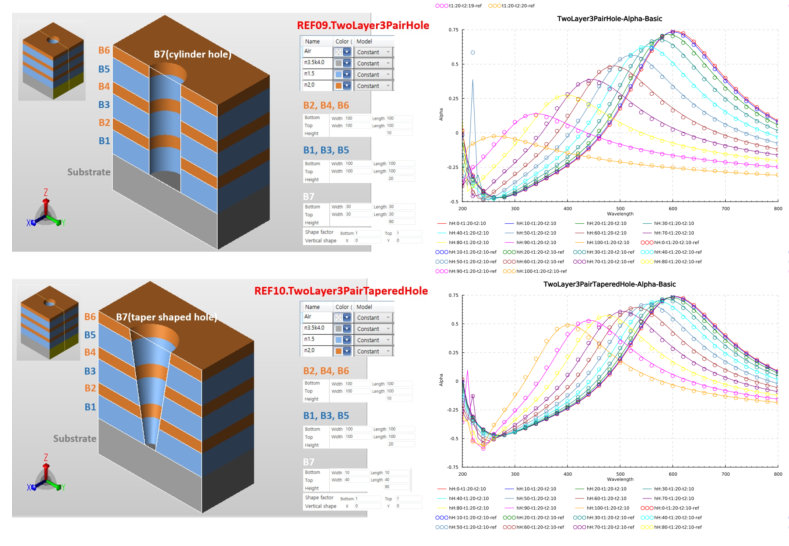
GPU-accelerated RCWA/FMM — reflection/transmission, Ψ/Δ, Jones, Mueller, Stokes S0–S7 for spectrum libraries & AI training.
mldosa — HPL
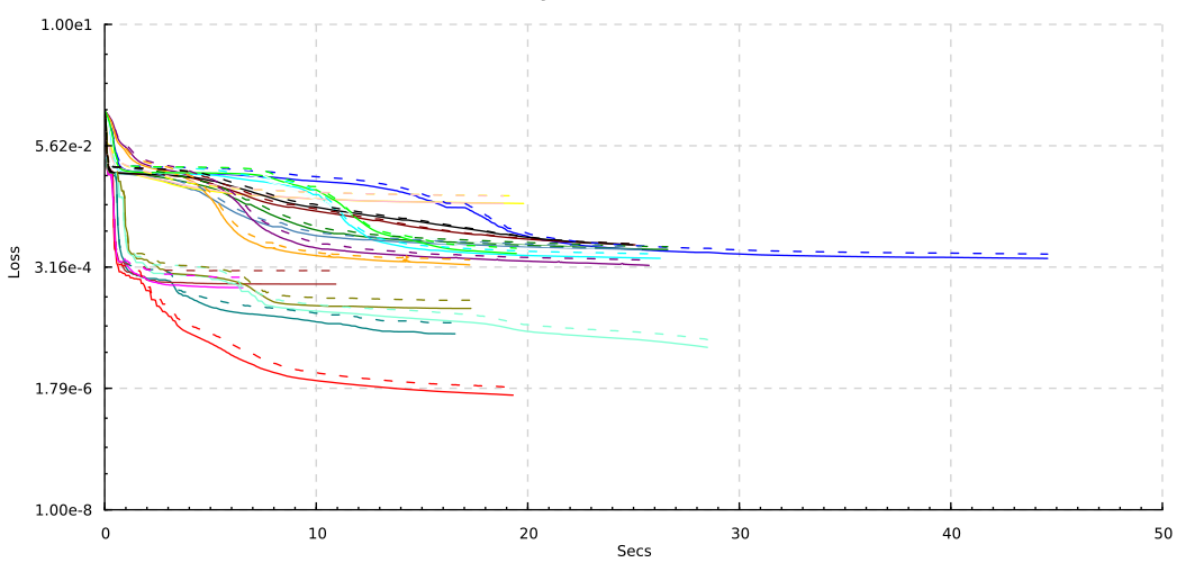
2nd-order GPU-accelerated High-Precision Learning — fast, accurate convergence on high-oscillation spectra and narrow responses.
Where rigor meets the real world.
Optical metrology
OCD/SE engines, RCWA/FMM analysis, metrology SW, high-precision ML — in-house engine, Hybrid-OCD research.
Inspection performance
Algorithm optimization, parallelization, CPU/GPU acceleration, takt-time improvement — drop-in modules.
Image AI
AI-AOI classification, unsupervised anomaly detection, segmentation, factory-automation integration.
3D metrology
Holotomography rendering, automatic geometry analysis, TGV/hole/bump inspection software.
Image stitching and processing
Tile registration, CPU/GPU parallel processing, accuracy validation — faster large-area reconstruction.
Process & spectrum
Spectrum analysis, wafer defect inspection, accumulated-data analysis & quality-judgment workflows.
A · T · K-Lab · national R&D · multiple industrial clients
Have a complex problem worth solving?
From initial consulting to full implementation, we navigate the complexity with you — and leave you with sustainable, reproducible solutions.